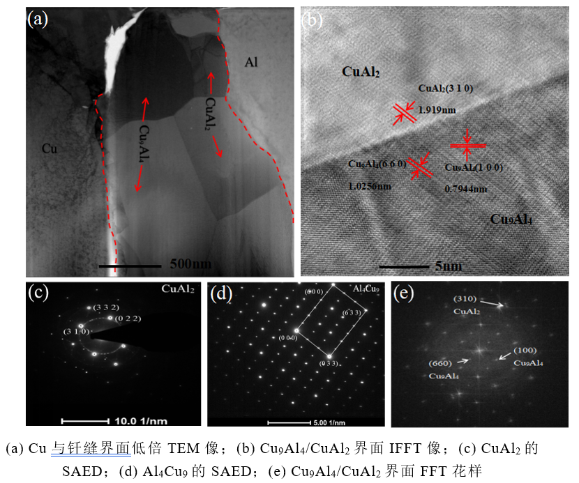
图2.57(a)为低倍TEM像,从图中可见紧邻Cu侧存在有大小不等的晶粒;图2.57(b)~(e)为图2.57(a)中不同微区的电子衍射花样。在近铜侧钎缝界面Cu母材与BAl88Si钎料之间存在两种反应产物,经过图2.57 (c)(d)SAED标定,两种金属间化合物分别是CuAl2与Cu9Al4。靠近Al侧反应层由Al衬底的CuAl2层组成,如图2.57 (a)所示,CuAl2首先成核,然后沿Al表面生长。高温钎料融掉的Cu母材表面,被推至液态钎料前沿,Cu元素在液态钎料中相互扩散,相互接触,形成连续的CuAl2层。图2.57 (b)为CuAl2与Cu9Al4界面的IFFT像,上侧为CuAl2金属间化合物,下侧为Cu9Al4金属间化合物。在对应HRTEM的FFT(图e)中经过标定衍射斑点,标出了Cu9Al4的(660)和(100)两个晶面与CuAl2的(310)晶面,两个平面的晶面间距dCuAl2(310)=1.919nm,dCu9Al4(660)=1.0256nm和dCu9Al4(100)=0.7944nm。为了分析CuAl2与Cu9Al4的晶体结合,可以根据方程(1)来评估晶体间的晶格失配度。
Fig. 2.57 (a) shows TEM images at low magnification. It can be seen that there are grains of different sizes on the side adjacent to Cu.Fig. 2.57 (b) ~ (e) shows the electron diffraction patterns of different micro-regions in Fig. 2.57 (a).There are two kinds of reaction products between Cu base metal and Bal88Si solder at the interface of brazing seam near copper side. According to SAED calibration in Fig. 2.57 (c)(d), the two intermetallic compounds are CuAl2 and Cu9Al4 respectively.The reaction layer near Al is composed of CuAl2 layer on Al substrate, as shown in Fig. 2.57 (a). CuAl2 first nucleates and then grows along the Al surface.The surface of Cu base metal melted by high temperature solder metal is pushed to the front of liquid solder metal, where Cu elements diffuse and contact each other to form a continuous CuAl2 layer.Fig. 2.57 (b) shows the IFFT image of CuAl2 and Cu9Al4 interface, with CuAl2 intermetallic compound on the upper side and Cu9Al4 intermetallic compound on the lower side.After calibrating diffraction spots in FFT(Fig. E) of corresponding HRTEM, two crystal planes (660) and (100) of Cu9Al4 and (310) of CuAl2 are marked. The spacing of crystal planes between the two planes is DCuAl2 (310)=1.919nm.DCu9Al4 (660) = 1.0256 nm and dCu9Al4 (100) = 0.7944 nm.In order to analyze the crystal bond between CuAl2 and Cu9Al4, the lattice mismatch between the crystals can be evaluated according to Equation (1).