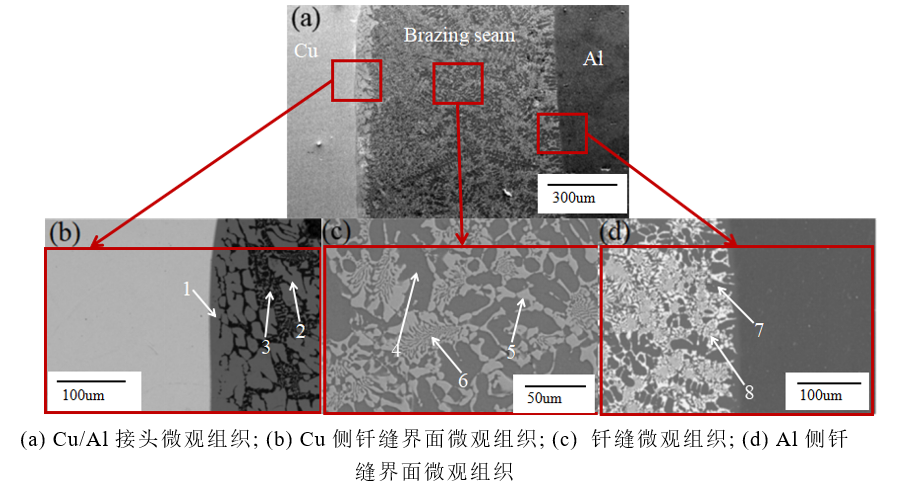
图2.51为Cu/BAl88Si/Al钎焊接头微观形貌SEM像,图(a)为低倍像,图中左侧为Cu母材、右侧为Al母材、Al-Cu之间形成有宽度为500um的钎缝。图2.51(b)~(d)为图2.51 (a)不同区域的放大像,从图2.51 (a)可知钎料与母材实现了良好的冶金结合,无裂纹形成;从图2.51 (b)可知在钎缝Cu侧界面形成了金属过渡层,灰黑色晶体以椭圆状状晶形式向钎缝内部生长;从图2.51 (d)可知在钎缝Al侧界面,亮白色晶体以树枝状垂直于钎缝向内生长;从图2.51 (c)可知灰色骨骼状晶体围着团状黑色晶体分布
Figure 2.51 is the SEM image of the Cu/BAl88Si/Al brazed joint. Figure (a) is a low-magnification image. The left side of the figure is the Cu base material, the right side is the Al base material, and the width between Al-Cu is formed. Brazing seam of 500um. Figure 2.51 (b) ~ (d) are enlarged images of different areas in Figure 2.51 (a). From Figure 2.51 (a), it can be seen that the solder and the base metal have achieved a good metallurgical bond without crack formation; from Figure 2.51 (b) It can be seen that a metal transition layer is formed on the Cu side interface of the brazing seam, and the gray-black crystals grow into the brazing seam in the form of elliptical crystals; from Figure 2.51 (d), it can be seen that at the Al side interface of the brazing seam, the bright white crystals are perpendicular to The brazing seam grows inward; from Figure 2.51 (c), it can be seen that the gray skeletal crystals are distributed around the mass of black crystals